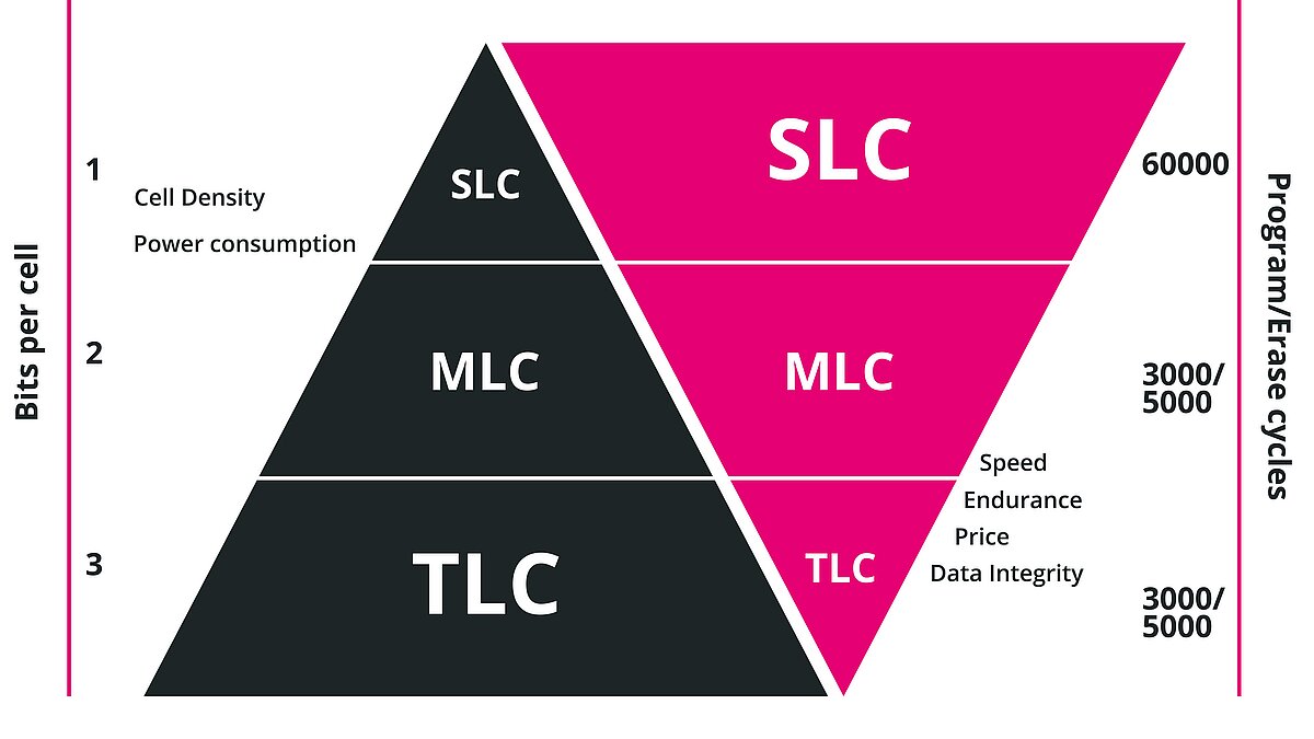
Figure 1: Bits per cell and P/E cycles of the SLC, MLC, and TLC technologies. [Taken from IM whitepaper]

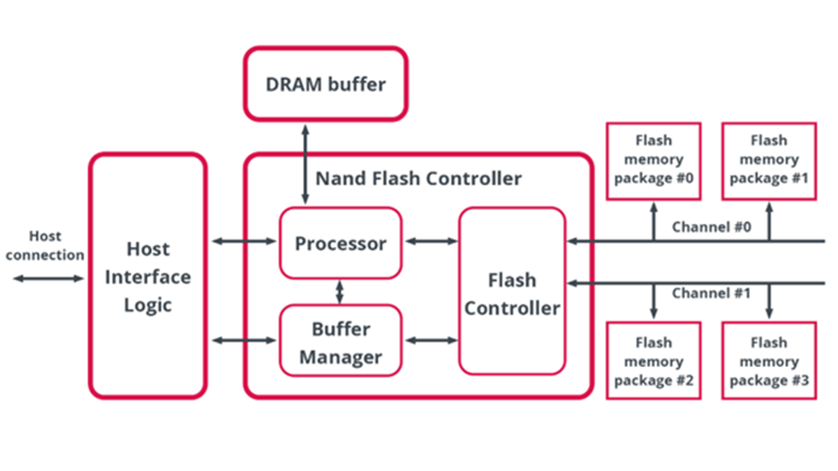
In NAND flash, the workload and write pattern, as well as the quality of the drive’s controller and firmware with operations can also affect the endurance of the drive (Figure 2).
Figure 2: The internal management of a NAND controller.

Limiting the Factors That Impact Endurance
The P/E cycle figure is calculated using only the blocks of new data to be written to the drive. Because of the way the NAND memory operates, there is always more data written to the drive than the supplied data. This is due to the data reshuffling that takes place within the NAND architecture, meaning that there are multiple writes happening for every write operation the user requests in the drive. The discrepancy between the data to be written to the drive, and the amount of data actually written in the process is known as the write amplification factor (WAF). Since the number of times the cells within a NAND flash can be written to is finite, the larger the WAF, the shorter the endurance. According to JEDEC, WAF is defined as the “data written to the flash divided by the data written by the host to the SSD,” as shown in Equation 1.
Equation 1: WAF = (Data written to NAND flash) / (Data written by host)
There are a number of algorithms the controller can use to optimize the WAF and improve endurance. These algorithms include over-provisioning, garbage collection, wear leveling and bad block mapping. In an ideal world, a WAF of 1 would demonstrate that the amount of data the entire system writes into the drive’s controller is precisely the same as the amount of data the controller writes into the drive’s NAND flash. In the real world, this never occurs. Methods used to increase endurance include:
Overprovisioning
Overprovisioning reserves spare flash blocks for use by the controller. The algorithm bypasses the tedious and time-consuming erase/write process that occurs when the flash must write even though an entire block has been used. This can involve reading new content, adding new content to cache, removing unused data from cache, erasing the addressed block in flash, copying the entire block from the cache, and emptying the cache. Instead of erasing the unavailable portion of the block to accommodate new data, the controller uses spare memory blocks.
Wear Leveling
Wear leveling distributes erase and writes across larger flash block sections to ensure the same memory blocks are not overwritten too often, limiting the risk that the entire drive’s life will be determined by a single, over-utilized block. Instead, all blocks should receive similar amounts of P/E cycles.
Garbage Collection (GC)
GC invalidates obsolete blocks and frees them up for write operations by selecting “victim” blocks — or blocks containing invalid sectors — and copying the valid information into other free sectors to finally erase the victim block. To minimize any impact of drive performance, this is often run in the background. GC efficiency is defined as the average number of invalid pages in each victim block to be erased. A high GC efficiency with more optimal victim selection (e.g., FIFO, Greedy, Windowed, etc.) improves the WAF.
Thermal Throttling
Another factor that can reduce endurance is that of high ambient temperature. The drive may experience some derating with any temperature increase, where overheating will cause poor data retention and reduce endurance. Thermal throttling addresses overheating by reducing drive speeds. This allows the chip to cool and mitigates the risk of part failure or device degradation.
The Importance of Accounting for Workload
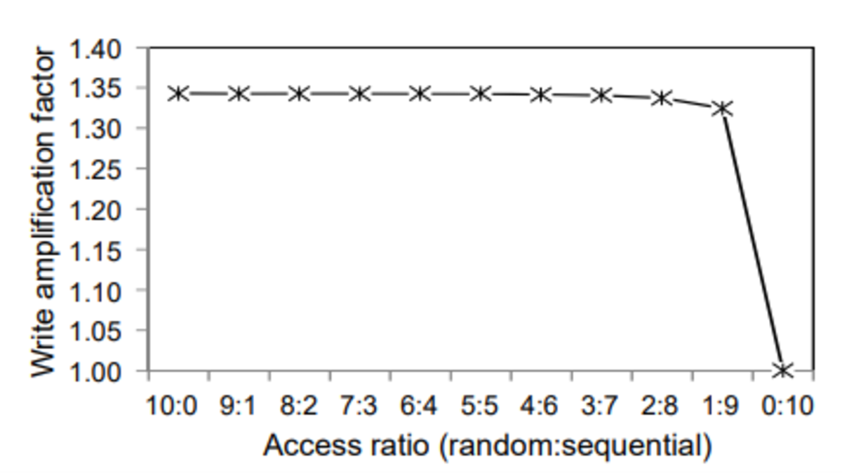
The endurance of the drive will also vary with the data stream from the host or the workload. These can either be sequential or random read/write accesses. It has been found that mixed workloads composed of mostly sequential write (with a small number of random writes) will drive up the WAF substantially and cause more wear than larger sequential writes (Figure 3).
Figure 3: The decrease in WAF to 1 when the ratio of random to sequential access goes from 10:0 to 0:10. Source: [1]

If the anticipated workload is sequential with no features that might cause the WAF to change over the device’s lifetime, many of the algorithms listed above may be unnecessary. However, if the workload is mainly sequential with regular random events, the algorithms will be continuously run in the background to optimize WAF. Workloads with different ratios of sequential to random writes will require much higher performance. In order to optimize both drive endurance and part cost, it is important to optimize specific features based upon the application. To gain a more realistic understanding of the drive’s longevity, WAF-based parameters such as drive writes per day (DWPD) and terabytes written (TBW) will be more accurate.
TBW and DWDP
JEDEC defines two main parameters to characterize endurance: TBW and DWPD. TBW is the number of terabytes that may be written to the drive over its lifetime and is defined by Equation 2.
Equation 2: TBW = ((Raw Capacity in GB) × (Program/Erase Cycles of the NAND)) / (WAF × Guardband ×1024)
As the equation shows, JEDEC suggests the use of a guardband to account for the effects of wear leveling or GC. This factor can be measured from similar drive data or estimated from the design of the wear leveling or GC schemes. It is necessary to use a simulated workload that is either defined by JEDEC or is application specific. NAND operates more efficiently when new, as existing blocks do not need to be deleted before writing, meaning that several write erase cycles should be performed until the memory reaches its operational steady state. WAF can be more accurately measured after the NAND flash has reached that steady state and does not need to be operated to its full endurance rating [2]. DWPD uses the TBW specification to calculate the number of times the user capacity of a drive can be written per day over the warranty period, or a different number of years.
Equation 3: DWPD = (TBW × 1024) / (User Capacity in GB × Number of Years × 365 Days)
As each application is different, it is difficult to provide a definitive example of a typical use cases. However, the figures below demonstrate how much the P/E cycles figure can differ from reality.
For example, a 3D-TLC flash, NAND flash device with a 128 GB capacity has an assumed 3,000 P/E Cycles, WAF of 3, 2% guardband and 3-year lifetime, which would give it a TBW of:
TBW = (128 GB × 3000 P/E Cycles) / (WAF 3 × 2% Guardband × 1024) = 62.5 TB
This is just a fraction of the endurance suggested by the P/E cycle figure. Using the same NAND flash, the DWPD figure would be:
DWPD = (62.5 TBW × 1024) / (128 GB × 3 years × 365 days) = 0.45
This means that the capacity of the drive could be written to merely 0.45 times each day.
In Practice
In the real world, NAND flash will be employed in a wide variety of applications where requirements will differ quite dramatically. For example, the SAS-attached read-intensive SSDs used in datacenters will often have a typical endurance of 1 DWPD, meaning that the full drive capacity can be written on it daily for its working life of five years. On the other hand, high performance computing (HPC) systems’ files may have write-intensive workloads that might call for a 5 to 10 DWPD over the device’s five-year lifetime.
The value of DWPD can go from 0.2 to beyond 10 in order to meet each application’s requirements. The factory default DWPD can also be increased by reserving percentages of the usable capacity for WAF lowering algorithms. A combination of solutions can be employed to save cost and maximize device lifetime, but this can only be accomplished once parameters such as TBW, DWPD, and WAF are known.
Summary
This article demonstrates why the endurance of a NAND flash device cannot truly be defined by P/E cycles, due mainly to the differences in workload. Sequential workloads will exhibit a WAF much closer to 1 than random workloads. The nature of the workload is highly dependent on the end application; algorithms that run in the background to maximize endurance may be necessary or completely unnecessary. It is therefore important to thoroughly understand the requirements of the NAND flash based upon the specific application and work from there. Datasheets that list WAF-based parameters such as TBW and DPDW offer much better insight into the drive’s endurance with dynamic workloads over P/E cycles. These are the parameters to look out for when choosing your next NAND flash.
Written and compiled by Alistair Winning and Anil Burra
References
[1] E. Lee, J. Kim, H. Bahn and S. H. Noh, "Reducing write amplification of flash storage through Cooperative Data Management with NVM," 2016 32nd Symposium on Mass Storage Systems and Technologies (MSST), Santa Clara, CA, USA, 2016, pp. 1-6, doi: 10.1109/MSST.2016.7897087.
[2] Cox, Alvin. "Compatibility Mode." JEDEC Solid State Drive (SSD) Specifications Explained. JEDEC Solid State Drive Joint Working Group, 2023. Web. https://www.jedec.org/sites/default/files/Alvin_Cox%20[Compatibility%20Mode]_0.pdf.

